

Introduction: Attiny85 Keyboard for Under $8!

This small keyboard was made with a few passive components, some blank PCB material, a buzzer, one LED, an Attiny85 and lots of love! The goal of the project was to make a keyboard that is fun and easy to make and that won't cost a fortune to make.
Step 1: Materials and Tools Required
I have added the prices of the costs of all of the items in some cases I had to buy quantities of more than one item at a time. I live in South Africa so I am simply going to convert the cost of each item based on the current exchange rate just to give an idea of how much this project is going to cost to make. Some items, such as the Arduino uno can be borrowed since it will only be used to flash the program onto the Attiny85 micro controller so I have excluded this from the cost of the keyboard.
- Toner transfer paper x 1 ($0.3)
- Attiny85 x 1 ($2)
- 1206 SMD LED x 1 ($0.2)
- 2k Resistors x 13 ($0.25)
- 1M resistor x 1 ($0.25)
- 47 Ohm resistor x 1 ($0.25)
- 0.1uF Capacitor x 1 ($0.07)
- 10uF Capacitor x 1 ($0.2)
- 3V passive buzzer x 1 ($0.3)
- 5V voltage regulator x 1 ($0.35)
- 9V battery x 1 ($1.75)
- 9V battery connector x 1 ($0.5)
- 1 pin male header x 1 ($0.25)
- Female to Male jumper wire x 1 ($0.1)
- Blank single sided PCB x 1 ($1.11)
Socket IC 8 Pin x 1 ($0.07)
The total cost of the materials is only $7.95!
Tools required
- A soldering Iron
- An iron
- A laserjet printer
- A permanent marker
- Ferric Chloride or any other etching chemical
- Sandpaper
- 0.6mm drill bit (it does not have to be exactly this size)
- A drill or rotary tool
- An Arduino Uno
- Male to male jumper wires
- A breadboard
- A PC or laptop that can run the Arduino IDE
- A USB cable for the Arduino
Step 2: Print the Design Onto the Toner Paper

For this step you simply need to print out the PDF that has been attached to this instructable onto your A4 sized toner transfer paper. This must be done with a laser printer and the print settings need to be on the highest possible dpi and darkest possible toner option! Be careful not to touch the ink after it has been printed since it falls off very easily! After the design has been printed you need to cut out the design as shown in the photo.
Attachments

Step 3: Preparing the Blank PCB

In this step, you are required to roughly cut the PCB to size. This can be cut with an iron saw, craft knife or any cutting method that you prefer as this cut does not need to be perfect. Measure out 75mm, which is half of the 150mm x 100mm PCB. Sand the PCB with around 400 to 800 grit sandpaper as shown in the photo above.
Step 4: Transfer the Design and Peel Off the Transfer Paper


For this step I used a type of industrial toaster in order to heat transfer the design onto the copper but I said one needs an iron do do this in the list of tools that are required. The same steps apply. One needs to place the design down onto the copper with the toner facing down (the toner needs to be touching the copper). Heat must then be applied for around 2 minutes (The iron must be on its highest heat setting). After two minutes the iron needs to rotated and pressed down for another minute to ensure that it transfers everywhere. After doing this, leave the board for a few minutes to cool off and place it in lukewarm water for around 10 minutes. The paper will already start to peel off on its own. One can now gently pull off the transfer paper. Some of the ink will not transfer correctly but this will be fixed in the next step.
Step 5: Fill in the Parts Where Ink Did Not Transfer

In this step a maker is required. Carefully will all of the parts where ink did not transfer correctly. One can also scratch off the parts the transferred incorrectly due to too much heat or pressure.
Step 6: Etch and Clean the Board


In this step I used Ferric Chloride to etch the board but there are many options that are available. It is very important that gloves are used during this step and that it is done in a well ventilated area! Dilute the ferric chloride with water and mix it with around a 1:1 ratio with the water. One must then leave it for around 10 to 15 minutes and constantly check if all of the excess copper has been removed from the PCB. Afterwards clean the board in a separate water bowl until it is clean. Please note that ferric chloride cannot be disposed of down the drain since it is very bad for the environment, it needs to be disposed of responsibly.
Step 7: Clean Up the Edges and Drill All of the Holes


For this step one needs to cut the board more accurately around the outline copped in the design and sand the edges with around 100 grit sandpaper in order to make the board more presentable. After this has been done one needs to drill all of the holes that have been transferred in order to prepare the board for painting and soldering. Please wear a particle mask and gloves while doing this as you are sanding fiberglass board which can be hazardous to your health! After the board has been tidied up one can start with the drilling process. Drill all the holes (preferably with some sort of drill press) and this step is now complete!
Step 8: (Optional) Paint the PCB

Paint the etched PCB with the spray paint colour of your choice. After painting simply sand the copper side of the pcb with 400 grit sandpaper and only the copper parts will be sanded since the rest of the board is lower than the copper.
Step 9: Solder Time!


First solder the SMD LED to the one side of the board. I have found its easiest when one first solders the pads alone and then place the SMD component to the pad with solder on it. Heat must then be applied with the soldering iron to one side of the LED and then heat on the other side in order to solder the component. I have indicated on the image above which way the small green dot on the LED must face Next we need to turn the board around and solder the rest of the components. I have added an image with labels on all of the components in the correct positions. Solder the components in the following order for it to be easiest; resistors, the 0.1uF capacitor, the IC socket, the voltage regulator, the buzzer and finally the single header pin. The schematic has been added above. The circuit is basically just a network of resistors which divide 5V op into 12 different values which is then read by a microcontroller which plays a certain tone through a buzzer.
Attachments
Step 10: Programing the Attiny85 and Adding the IC


This is the final step! After this has been done the IC can be places in the socket, jumper can be connected and finally the battery can be connected and its ready to play! This step is however the most complicated so the steps need to be replicated exactly. For starters Arduino 1.6.4 needs to be downloaded and can be downloaded from this link;
https://www.arduino.cc/en/Main/OldSoftwareReleases... select version 1.6.4 of the required operating system.
Open the code that has been attached to this instructable labeled "Keys".
Next we need to Go to preferences, under file as shown in an image above and paste the following link where it says "Additional Boards Manager URLs"
http://drazzy.com/package_drazzy.com_index.json
Next we need to install the board under the boards manager tab as shown in the image above.
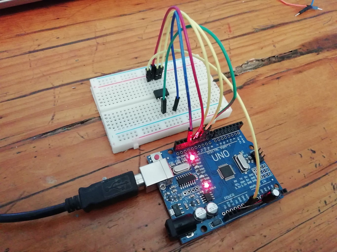
The Attiny85 can then be placed in the breadboard as shown above. The 10uF capacitor needs to connected to the reset and ground pins on the Arduino Uno. Ground and 5V from the arduino need to be connected to pins 4 and 8 respectively on the Attiny85. Arduino Pin 13 must be connected to Attiny85 pin 2. Arduino Pin 12 must be connected to Attiny85 pin 1. Arduino Pin 11 must be connected to Attiny85 pin 0 and Arduino pin 10 needs to be connected to Attiny pin 1.
Select the Attiny25/45/85 as the board. Attiny85 as the chip, 8Mhz (internal) as the clock, and keep the rest of the options as they are. now make the programmer "Arduino as ISP".
Next we can press upload and just like that the Attiny85 has been programmed!
Highlowtech has a wonderful article on this that explains everything much better than I can, the link for that is;
http://highlowtech.org/?p=1706
The Attiny85 can now be placed in the IC socket on the soldered PCB. The orientation is very important! The side of the IC with the small dot on it must face to the left of the board.
Attachments

Step 11: Time to Play!
Plug in the battery and jumper wire and let your imagination go wild! Just excuse my terrible playing.

Participated in the
Audio Contest 2018


