Introduction: How to Use Verilog and Basys 3 to Do 3 Bit Binary Counter


I have done this project for an online class. The project is written by Verilog. The clock divider and counter modules were provided. My task was to write the top module to display 3 bit output of the counter on the 7 segment display. Originally, the project was implemented in Basys 2. I also used Xilinx ISE Webpack. Now, I modified the counter module and top module and implemented it on Basys 3. In addition, I used Vivado Webpack instead of ISE. I have also written up a getting started guide for Vivado.
Step 1: Step 1: Install Xilinx Vivado Webpack
I got the Vivado Webpack 2014.3 before and upgraded to Vivado 2015.2. If you haven’t got Vivado, please look at the getting started guide and get one for free.
Step 2: Step 2: Create a New Project


You can follow the getting started guide to create a new project. However, I will still go through that very briefly.
First, open Vivado Webpack. Thenclick “Create New Project”
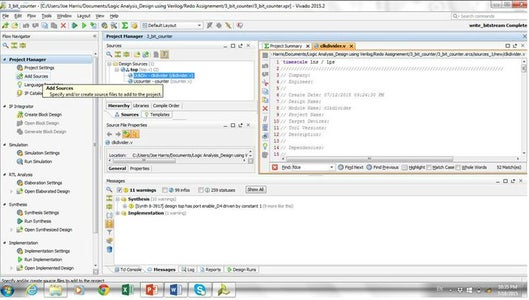
Click “Next”. Name the the project and choose the project location. I name the project as 3_bit_counter and put that under my C drive
Click “Next” and choose the project. We choose a RTL project. RTL is called register transfer level.
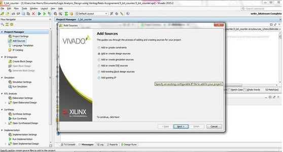
Click “Next” and then add sources. As we don’t have any pre-built module, so we just click “+” and create file
Choose file type Verilog and name it as “clkdivider”. We will have three modules – clock divider, counter and top moudle. The counter and top module will be created later.
Click “OK” and you will see a “clkdivider” file has been created
Click “Next” as we don’t have any IP in the project
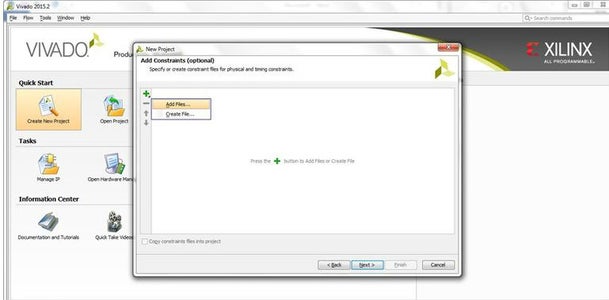
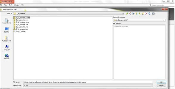
Click “+” to add constraints in the project. You can download the Basys 3 master xdc file from Digilent. Click “Add File” and then find out where you save the master xdc file. In this case, I saved under the file under the 3_bit_counter project
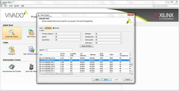
Choose the right device. The Xilinx FPGA device on Basys 3 is Artix 7 a35T. The package is cpg236. The temp grade is C and speed grade is -1. You can use the filter to find out the right device.
Click “Next” to check everything in the project summary. If it is correct, click “Finish”. Then, the new project is created
Step 3: Step 3: Create Clock Divider
The clock speed for Basys 3 is 100MHz. However, we don’t need the full speed in the project. We write a clock divider to get two slower clocks (380 Hz and 190 Hz). To do that, we use the library functions (D Flip-Flop with Clock Enable and Asynchronous Clear). You can find out the primitive in the Xilinx Vivado Tutorial. We instantiate as many FDCE as we want to have the desired clock speed.
In the module, the input is the master clock on Basys 3 and outputs are clock speed we want.
You can see the code with comments in the project file.
Step 4: Step 4: Create Counter Module
We need to add sources. Go to the Flow Navigator and click “Add Resources”
Then, choose “Add or create design resources” and next. This will bring you to add or create files interface. Just follow what we did in step 2 to create a verilog file. You can key in inputs or outputs. Or, you just ignore it and do that when you write the code.
Once you have created the file, we can write the counter logic. The input is the clock speed to drive the counter and outputs are 3 bits in the counter – Q1, Q2 and Q3.
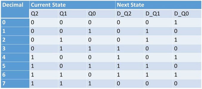
Basically, the counter will count from 0 to 7 in decimal (2^3 -1). So, we have current and next states. The current state is the bit stored in the register currently and next state is the bit which will be put into the register when the clock reach the positive edge.
The curent state is the output Q while we name variables for next state D0, D1 and D2
So, we can describe the current and next state logic as follows. When we finish counting 7, the counter will go back to 0. (see the table)
We can use K-map to generate the logic equation for each bit in the next state. Then, we use the flip-flop (FDCE library function) to generate output.
Note: you can use the behavioral state to write the counter logic. There is an example in Digilent learn site: https://learn.digilentinc.com/Documents/262
You can find the detailed code with comments in the project file.
Step 5: Step 5: Create Top Module


Follow the step 4 to add a top module. Then, we need define inputs and outputs that connect to the external environment. The only input is the clock from Basys 3. There are three types of output, enable_Dx,cx and dp. The enable_Dx is the power to each 7 segment display digit. There are total 4 in Basys 3. However, we only need 3. The cx is the segment connection. In each digit, there are seven segments from ca to cg. The dp is the decimal point on the display. We don’t need to use dp in the project.
Input:
clk // master clock for Basys 3
Outputs:
enable_D1,//right most digit
enable_D2
enable_D3,
enable_D4,//left most digit
ca,cb,cc,cd,ce,cf,cg // segment connections
dp // decimal point
We also need the following variables to instantiate the clock divider and control how fast the digit is on and off. All of them are net variables.
clkout1; //internal signal for the divided clock output
clkout2; //internal signal for the divided clock output
clkOut; // internal signal for the divided clock output
Q0,Q1,Q2; // internal signal for the counter output
wire n,o,p; //internal signal to control the on / off of 3 digits
Then, we use the gate level function to control on and off of the digit. The digit is common anode. The FPGA pin for the digit is connected as output while a constant 3.3V is supplied as input in the LED. To turn on the digit, we need to drive the pin low (active low). You can find the details at Basys 3 reference manual. We never use left most digit enable_D4, so we assign it to constant 1’b1. Then, we use the and and not gate function to make the digit on and off based on the clk generated from clkdivider
assign enable_D4 = 1'b1; //turn off the left most digit which is D4
and U1 (n,clkout2,clkout1); // use AND gate to turn on and off the digit so that only one digit is on at a time
and U2 (o,clkout2,~clkout1); // use AND gate to turn on and off the Digit so that only one digit is on at a time
and U3 (p,~clkout2,clkout1); // use AND gate to turn on and off the Digit so that only one digit is on at a time
not (enable_D1,n); // n = clkout2 & clkout1, enable_D1 is low (on) when both clkout2 and clkout1 is high
not (enable_D2,o); // o = clkout2 & ~clkout1, enable_D2 is low (on) when clkouut2 is high and clkcout1 is low
not (enable_D3,p); // p = ~clkout2 & clkout1, enable_D3 is low (on) when clkout2 is low and clkout1 is high
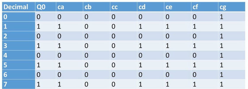
After that, we decide the logic for the seven segment in each digit. Same as enable_Dx, cx is active low signal. So, to turn on the segment, we need to drive the FPGA to low. Here are the truth tables for the Qx (Q2,Q1,Q0) and ca-cg (see tables)
From the truth table, we can have the following conclusion
cb and cc are always 0
cg is always 1
ca,cd,ce and cf always have the same output
value of ca is evaluated by Qx
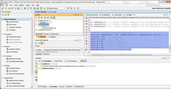
Therefore, we can have the following assignment. For, cb-cg, it is pretty stragightforward. For ca, we use nest coniditional operator to evaluate the enable_Dx to decide the output of the ca. If enable_D1 is on, which means the left most digit (Q0) is on, from the truth table, ca will be Q0. Otherwise, we need to evaluate the other condition (enable_D2 is on). If enable_D2 is on, then ca is equal to Q2 and so on.
assign ca = (enable_D1==0) ? Q0: ((enable_D2==0)? Q1: ((enable_D3==0) ? Q2:1'b1)); //use conditional operator
assign cb = 1'b0; // cb is always on
assign cc = 1'b0; // cc is always on
assign cd = ca; //cd output is same as ca
assign ce = ca; //ce output is same as ca
assign cf = ca; //cf output is same as ca
assign cg = 1'b1; // as we only need to have zero or one, so cg is off all times
assign dp = 1'b1; //turn off the decimal point
Finally, we need to instantiate the clkdivider and counter module.
You can find the code with comments in the project file.
Step 6: Step 6: Modify the Constraint File
We need to uncomment ports we want to use in the physical hardware and change the port name to match the name in our module. As mentioned before, we need clk, enable_Dx, cx and dp as input and outputs. So, we need to first find these ports in the master xdc.
Expand the constraints in the sources panel
Double click the Basys3_master.xdc. Then, you see codes describing all physical input and output properties. When we delete “##”, the statements will be un-commented so that we can use these pins. All FPGA pins in the master xdc are grouped under the same peripheral. For example, if you want to find out pins for seven segment display, just click “ctrl+F” and then type “7 segment display” you will find out all pins including digit enables and segment connections. Rename the used ports (in each line, after get_ports) according to the top level signal names in the project
Step 7: Step 7: Synthesize the Design


Highlight “top module” in the source panel. Synthesize the design. Go to the flow navigator to click “Run Synthesis”.
Click the message tab to see any warning or error. In this project, there are warnings assignment for cx to the constant. You can ignore them as it won’t affect the implementation.
Step 8: Step 8: Implement the Design
Once you have successfully run the synthesis, there will be pop up to ask you to run the implementation. Click “OK” to continue. And same as step 7. Click “message” tab to see any warning or error.
Step 9: Step 9: Generate the Bitstream
Once you have successfully implemented the project, you can create the bitstream file.
Step 10: Step 10: Target the Hardware
Once the bitstream file has been created, the Vivado will ask you to connect the hardware. So, you connect the Basys 3 to the USB port of the computer. Turn it on and then click “open target”. You can choose auto connect or open new target. Then, the FPGA device will be detected. You can program the bitstream file to the block RAM through JTAG USB port at Basys 3 or SPI flash. In this case, we will use the JTAG USB port and Black RAM.
Step 11: Step 11: Program the Device
When you hit program the device, the done LED light on Basys 3 will be off. If the programming is successful, it will be back on. The on and off time varies depending on the size of project. Now, we will use 3 bit counter running from 000 to 111 and then back to 000.